Quick Answer
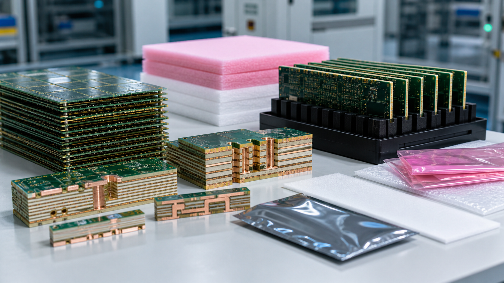
A multi-layer PCB manufacturer builds printed circuit boards with three or more conductive copper layers separated by insulating materials. Buyers use multi-layer boards when routing density, impedance control, power integrity, shielding or product size cannot be handled by a simple single-layer or two-layer PCB.
How Buyers Should Read This Topic
The key buying risk is not only whether the supplier can laminate several layers. The supplier must control stackup, dielectric thickness, copper weight, via quality, registration, surface finish and panelization so the finished PCB can be assembled reliably.
KEEP BEST connects this work through PCBA manufacturing services, quality management, DFM engineering support, RFQ review, OEM manufacturing, ODM engineering support, box build assembly and industry solutions so buyers can review manufacturing, engineering, quality and delivery boundaries before pricing is locked.
Buyer Checklist
1. Confirm the layer count, stackup, dielectric material, copper weight and finished board thickness.
2. Define controlled impedance requirements and ask how coupons or measurements will be handled.
3. Review via type, annular ring, aspect ratio, drill tolerance and plating reliability.
4. Check surface finish, solder mask, warpage risk and panelization for SMT assembly.
5. Align DFM feedback before the buyer releases pilot or production quantities.
6. Connect PCB fabrication assumptions to PCBA assembly, test access and rework limits.
Supplier Evidence Table
| RFQ area | Evidence to request | Why it matters | |---|---|---| | Stackup | Layer order, dielectric and copper confirmation | Protects electrical performance | | Impedance | Target values and verification method | Reduces signal integrity risk | | Via | Drill and plating capability | Protects reliability under thermal stress | | Panel | Panelization and fiducial plan | Improves SMT assembly yield | | Quality | Inspection and outgoing report | Supports buyer approval |
RFQ Questions to Ask
- Can the supplier confirm the exact stackup before fabrication?
- How will impedance be verified and reported?
- Which via structures increase cost or reliability risk?
- Will panelization support the assembly process?
- What fabrication tolerance may affect PCBA test or fit?
Practical Recommendation
Choose a multi-layer PCB supplier by evidence, not only by layer-count claims. Ask for stackup confirmation, impedance plan, via capability and assembly-aware DFM before the order is released.
FAQ
When should a product use a multi-layer PCB?
Use it when routing density, power integrity, signal integrity or product size cannot be solved with fewer layers.
Is a higher layer count always better?
No. Higher layer count can add cost and manufacturing risk. The stackup should match electrical and mechanical needs.
Should PCB fabrication and PCBA be quoted together?
For complex boards, quoting them together helps expose assembly, panelization and test-access risks earlier.