AI Compute PCBA Manufacturing, ODM/OEM and Testing Solution
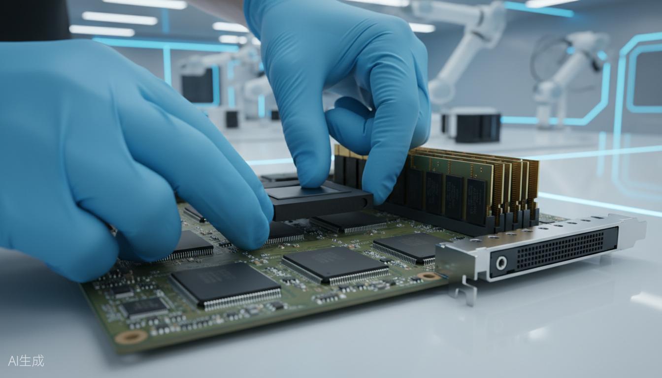
For AI compute cards and GPU server boards, Keep Best handles GPU/DDR thermal mismatch, high joint counts, nitrogen reflow and SPI/AOI/X-ray inspection loops.
Key definition
AI Compute solutions apply one-stop PCBA manufacturing, ODM/OEM transfer, SMT process control, testing, traceability and box build integration to this industry.
Key facts
- Step Stencil Design: Zoned thickness control by package thermal capacity and paste demand.
- GPU/DDR Reflow Window: Profile setup based on component temperature limit and soldering needs.
- 3D SPI/AOI/X-Ray: Paste, visible defect and BGA internal-joint risk coverage.
- Dense SMT: High component count, high solder-joint count and high-speed board introduction.
- Pilot-to-Volume Lock: Convert two pilot batches into repeatable SOPs and traceability records.
- Covers high-reliability scenarios including security electronics, IoT, industrial, new energy, medical and robotics
Engineering constraints and manufacturing risks
Thermal-Capacity Gap Between GPU and DDR
Very High SMT Joint Count
High Rework Cost for Premium Components
Pilot Process Must Be Repeatable
Typical products and validation points
AI Compute / Accelerator Card
Server GPU Board
Edge AI Compute Module
AI Vision Processing Board
High-End Graphics Control Board
SMT/PCBA process control matrix
High-Density SMT Assembly Scale
GPU/DDR Thermal-Capacity Gap
Step Stencil Paste-Volume Control
Reflow Profile and Nitrogen Reflow
Three-Layer Inspection Loop
Engineering path and volume delivery
Package and Thermal-Capacity Review
Step Stencil Design
Reflow Window Setup
Three-Layer Inspection Loop
Pilot Parameter Lock
Industry FAQ
Why do AI compute cards need a step stencil?
GPU and DDR require different paste volumes. Step stencil design gives the GPU area enough paste while controlling DDR paste volume to reduce bridging and collapse risk.
What does nitrogen reflow solve here?
Nitrogen reflow reduces oxidation and improves wetting, allowing more stable GPU soldering within a controlled peak temperature window while reducing DDR overheating risk.
How are X-ray focus areas defined?
Focus areas usually include GPU, DDR, PMIC and other high-value BGA devices, checking internal bridging, voiding, offset and cold solder risk.