Quick Answer
An HDI PCB manufacturer should help buyers select materials based on assembly reliability, not only board density. The RFQ should define layer count, microvia structure, dielectric thickness, Tg, CTE, copper weight, impedance needs, surface finish, thermal load, soldering profile and inspection evidence. Good material selection reduces via reliability risk, warpage, soldering defects and field failures after PCBA assembly.
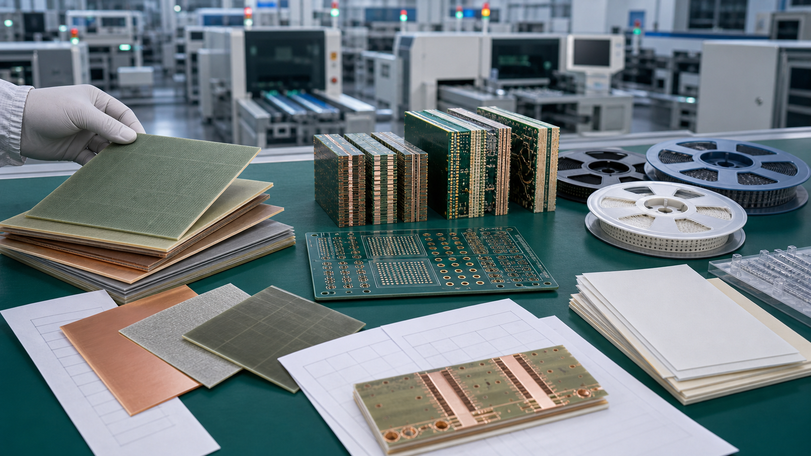
What HDI PCB Material Selection Means
HDI PCB material selection is the process of matching laminate, copper, build-up structure and surface finish to the electrical, thermal and assembly requirements of a high-density board. HDI designs often use microvias, thin dielectrics, fine traces, tight impedance control, BGA fan-out and stacked or staggered via structures. These choices affect both PCB fabrication and SMT assembly.
For buyers, material selection should connect PCBA manufacturing services, DFM engineering support, quality management, RFQ submission, OEM manufacturing, ODM engineering, box build assembly and industry PCBA solutions.
Why Material Choice Affects PCBA Reliability
HDI boards can fail when material assumptions are separated from assembly reality. A laminate may support fine routing but still create warpage, poor thermal balance, via fatigue, delamination or soldering instability if the assembly process is not considered. A buyer should ask the HDI PCB manufacturer and the PCBA factory to review the stack-up together before release.
This is especially important for BGA, fine-pitch connectors, RF sections, medical electronics, industrial controls and compact modules. Material decisions should be reviewed together with the DFM report issues closure guide, SMT panelization rails and fiducials guide and 0201 and 01005 SMT assembly process requirements.
Material Selection Checklist
1. Tg and Thermal Stability
Tg should match reflow exposure, operating temperature and expected reliability life. Higher Tg is not automatically better for every board, but the selected laminate must tolerate the soldering profile and product environment.
2. CTE and Z-Axis Reliability
Coefficient of thermal expansion matters for plated vias and microvias. A mismatch between material expansion and copper structure can increase barrel cracking, microvia fatigue or layer separation risk after thermal cycling.
3. Dielectric Thickness and Impedance
Thin dielectrics enable density and impedance control, but they also tighten fabrication tolerance. The buyer should confirm impedance requirements, test coupons and acceptable tolerance before releasing the PCB stack-up.
4. Copper Weight and Fine-Line Capability
Copper thickness affects current capacity, etching control, trace width, spacing and thermal behavior. Dense HDI layouts may need a balance between fine-line routing and copper robustness.
5. Microvia Structure
The manufacturer should confirm whether microvias are blind, buried, stacked or staggered. Stacked structures require stronger process control and reliability evidence. Buyers should ask for cross-section or reliability data when risk is high.
6. Surface Finish
ENIG, ENEPIG, OSP and immersion silver each have tradeoffs for solderability, shelf life, wire bonding, contact reliability and cost. The selected finish should match component mix, storage time and assembly process.
7. Laminate Loss and RF Needs
For high-speed or RF sections, dielectric constant, dissipation factor and material consistency matter. These properties should be defined before layout and verified with the board supplier where relevant.
8. Assembly Process Fit
The material plan should support panel stability, stencil printing, reflow profile, AOI, X-ray and rework boundaries. Material selection is not complete until assembly constraints are reviewed.
Buyer Evidence Table
| Decision area | Evidence to request | Reliability risk if missing | |---|---|---| | Stack-up | Controlled stack-up and material list | Wrong impedance or unstable fabrication | | Tg and CTE | Laminate data and reflow compatibility | Delamination or via fatigue | | Microvias | Structure, cross-section and process notes | Hidden via reliability risk | | Copper | Copper weight and fine-line capability | Etch variation or thermal imbalance | | Surface finish | Finish choice and storage guidance | Solderability or contact reliability issue | | Panel plan | Rails, fiducials and support strategy | Warpage or placement offset | | Inspection | AOI, X-ray and test coupon plan | Defects escape into assembly | | Release records | Lot, test and shipment records | Weak traceability after delivery |
RFQ Questions for an HDI PCB Manufacturer
- Which laminate series and stack-up are recommended for this density and reflow profile?
- Are microvias stacked, staggered, blind or buried, and what evidence supports the choice?
- What impedance tolerance and test coupon plan will be used?
- Does the board require ENIG, ENEPIG, OSP or another finish based on component mix?
- How will panelization and warpage be controlled during SMT assembly?
- What X-ray, cross-section or reliability evidence can be provided?
- What open DFM risks should be closed before PCBA production release?
Practical Recommendation
Do not treat HDI material selection as a PCB-only decision. The selected material must survive fabrication, SMT assembly, test, rework limits, product environment and shipment. The best supplier response should connect material data, stack-up control, DFM comments, test coupons and PCBA release evidence in one clear package.
FAQ
Is high Tg always required for HDI PCB assembly?
No. High Tg can be useful, but the correct choice depends on reflow exposure, operating temperature, stack-up, via structure and reliability requirements.
Is ENIG the default surface finish for HDI boards?
ENIG is common, but not always the best answer. ENEPIG, OSP or other finishes may be better depending on shelf life, contact needs, wire bonding, cost and assembly process.
Why do microvias need special evidence?
Microvias concentrate thermal and mechanical stress in small structures. Stacked microvias especially need process control and reliability evidence.
Should the PCBA factory review the PCB material plan?
Yes. Assembly constraints such as panel stability, reflow, X-ray visibility and rework limits should be reviewed before PCB release.
What should be included in the RFQ package?
Include stack-up, target impedance, material preference, copper weight, finish, microvia structure, Gerber, BOM, placement data, test requirements and reliability expectations.