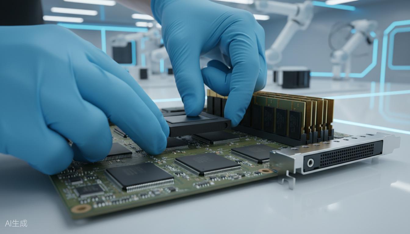
AI Compute
For AI compute cards and GPU server boards, Keep Best handles GPU/DDR thermal mismatch, high joint counts, nitrogen reflow and SPI/AOI/X-ray inspection loops.
ENGINEERING CONSTRAINTS
Engineering Constraints
Define manufacturing, testing, certification and delivery boundaries before building a verifiable engineering path.
Thermal-Capacity Gap Between GPU and DDR
The GPU package is large with many BGA balls and high thermal capacity. DDR packages are smaller with a narrow thermal window. The same reflow process must provide enough heat for the GPU while avoiding DDR bridging.
Very High SMT Joint Count
A typical AI compute card can contain 85 component types, 4,000 components and 9,200 SMT joints. Paste, placement or reflow drift can quickly become a yield issue.
High Rework Cost for Premium Components
GPU, DDR and high-speed connectors are costly. Rework affects not only material cost but also board reliability and customer delivery schedules.
Pilot Process Must Be Repeatable
AI server and accelerator-card customers expect the process parameters from pilot batches to become stable SOPs for continuing volume orders.
PRODUCT ARCHITECTURES
Product Architectures & Validation Points
Key process, testing and reliability points by product architecture.
AI Compute / Accelerator Card
Large GPU BGA, DDR memory, high-speed interface, step stencil, SPI/AOI/X-ray full inspection
Server GPU Board
Multiple BGA devices, thick-copper power layers, nitrogen reflow, BGA voiding and bridging inspection
Edge AI Compute Module
SoC plus BGA memory, PCIe/M.2 interface, low-power supply and functional burn-in
AI Vision Processing Board
High-speed imaging interface, DDR cache, GPU/FPGA collaboration and EMC pre-assessment
High-End Graphics Control Board
Large-area BGA, power network, thermal-structure coordination and batch traceability
SMT / PCBA PROCESS PARAMETERS
SMT/PCBA Process Parameters & Validation Matrix
Process windows, control limits, test coverage and traceability requirements are defined during engineering review, not only after a case is completed.
01
High-Density SMT Assembly Scale
Parameters / Limits
The AI compute card case includes 85 component types, 4,000 components and 9,200 SMT joints, with GPU, DDR and high-speed connectors concentrated on a high-value board.
Validation / Traceability
During NPI, solder paste, placement, reflow and inspection strategies are split by device type; pilot builds lock a repeatable process window.
02
GPU/DDR Thermal-Capacity Gap
Parameters / Limits
The GPU package is about 62.5 mm² with 3,700+ BGA balls and high thermal mass. DDR BGA has about 440 balls and lower thermal mass, making overheating and bridging a key risk.
Validation / Traceability
The DDR temperature limit defines the peak-temperature boundary, while X-ray validates GPU/DDR bridging, voiding and offset.
03
Step Stencil Paste-Volume Control
Parameters / Limits
The GPU area uses a 0.14 mm stencil thickness, while DDR and other areas remain at 0.12 mm to balance large-device paste volume with small-BGA bridging control.
Validation / Traceability
100% 3D SPI before reflow checks paste height, area and offset; results outside the window trigger line-side action.
04
Reflow Profile and Nitrogen Reflow
Parameters / Limits
The profile uses a 235-240°C peak-temperature window and time above liquidus (TAL) control, extending effective wetting time at a controlled peak temperature. Nitrogen reflow improves solder wetting.
Validation / Traceability
Each pilot batch records the reflow profile, while post-reflow AOI and X-ray validate visible and internal BGA solder quality.
05
Three-Layer Inspection Loop
Parameters / Limits
High-value GPU/DDR boards combine pre-reflow SPI, post-reflow AOI and X-ray inspection of BGA areas.
Validation / Traceability
SPI, AOI and X-ray are all 100% inspections; after two pilot batches, inspection windows and exception criteria are converted into volume-order standards.
ENGINEERING PATH
Engineering Path
From requirement review, DFM/DFT and process development to validation and traceable delivery.
Package and Thermal-Capacity Review
Confirm package, thermal capacity and soldering risk for GPU, DDR, PMIC, high-speed connectors and power devices.
Step Stencil Design
Design zoned stencil thickness according to GPU and DDR solder-paste needs, balancing large-BGA wetting and small-BGA bridging risk.
Reflow Window Setup
Use DDR temperature limits as the boundary while extending time above liquidus to provide enough heat for GPU soldering.
Three-Layer Inspection Loop
Use 100% 3D SPI before reflow, AOI after reflow for surrounding components, and X-ray for GPU/DDR internal solder joints.
Pilot Parameter Lock
Lock stencil, profile, inspection criteria, rework rules and MES records into volume-production SOPs.
KEY CAPABILITIES
Key Capabilities
Key capabilities providing end-to-end professional services for this industry.
Step Stencil Design
Zoned thickness control by package thermal capacity and paste demand.
GPU/DDR Reflow Window
Profile setup based on component temperature limit and soldering needs.
3D SPI/AOI/X-Ray
Paste, visible defect and BGA internal-joint risk coverage.
Dense SMT
High component count, high solder-joint count and high-speed board introduction.
Pilot-to-Volume Lock
Convert two pilot batches into repeatable SOPs and traceability records.
ENGINEERING VALIDATION CASES
Engineering Validation Cases
Capability boundaries shown through constraints, engineering response and validated results.
Two-Batch Pilot Introduction for High-End AI Compute Card
Constraint
The customer product served AI accelerator, AI server and graphics-card scenarios. The GPU supported large-model workloads. The board integrated 85 component types, 4,000 components and 9,200 SMT joints, with a large GPU BGA and smaller DDR BGAs on the same reflow process.
Engineering Response
Keep Best used a step stencil: 0.14 mm in the GPU area and 0.12 mm in DDR/other areas. The reflow profile used the DDR 235-240°C temperature limit as a boundary while extending TAL. Nitrogen reflow improved wetting, and 3D SPI, AOI and X-ray provided layered inspection.
Validated Result
Two pilot batches were delivered with stable quality. The process addressed GPU solder volume, DDR overheating/bridging and hidden BGA defect detection, leading to continuing volume orders.
Inspection Strategy Lock for GPU/DDR Mixed Board
Constraint
The customer needed evidence that internal BGA solder risks were controlled across batches, rather than relying on visual inspection alone.
Engineering Response
Keep Best split SPI, AOI and X-ray checks into process nodes and built focused inspection rules plus exception review for GPU/DDR key areas.
Validated Result
Inspection moved from a single check to a prevention, process and internal-defect loop, providing auditable evidence for volume delivery.
FREQUENTLY ASKED QUESTIONS
FAQ
Frequently asked questions about this industry solution.
Contact EngineersGPU and DDR require different paste volumes. Step stencil design gives the GPU area enough paste while controlling DDR paste volume to reduce bridging and collapse risk.
Nitrogen reflow reduces oxidation and improves wetting, allowing more stable GPU soldering within a controlled peak temperature window while reducing DDR overheating risk.
Focus areas usually include GPU, DDR, PMIC and other high-value BGA devices, checking internal bridging, voiding, offset and cold solder risk.

Ready to Start Your AI Compute Project?
No matter what stage you are at, Keep Best can provide matching PCBA manufacturing solutions.