Direct Answer
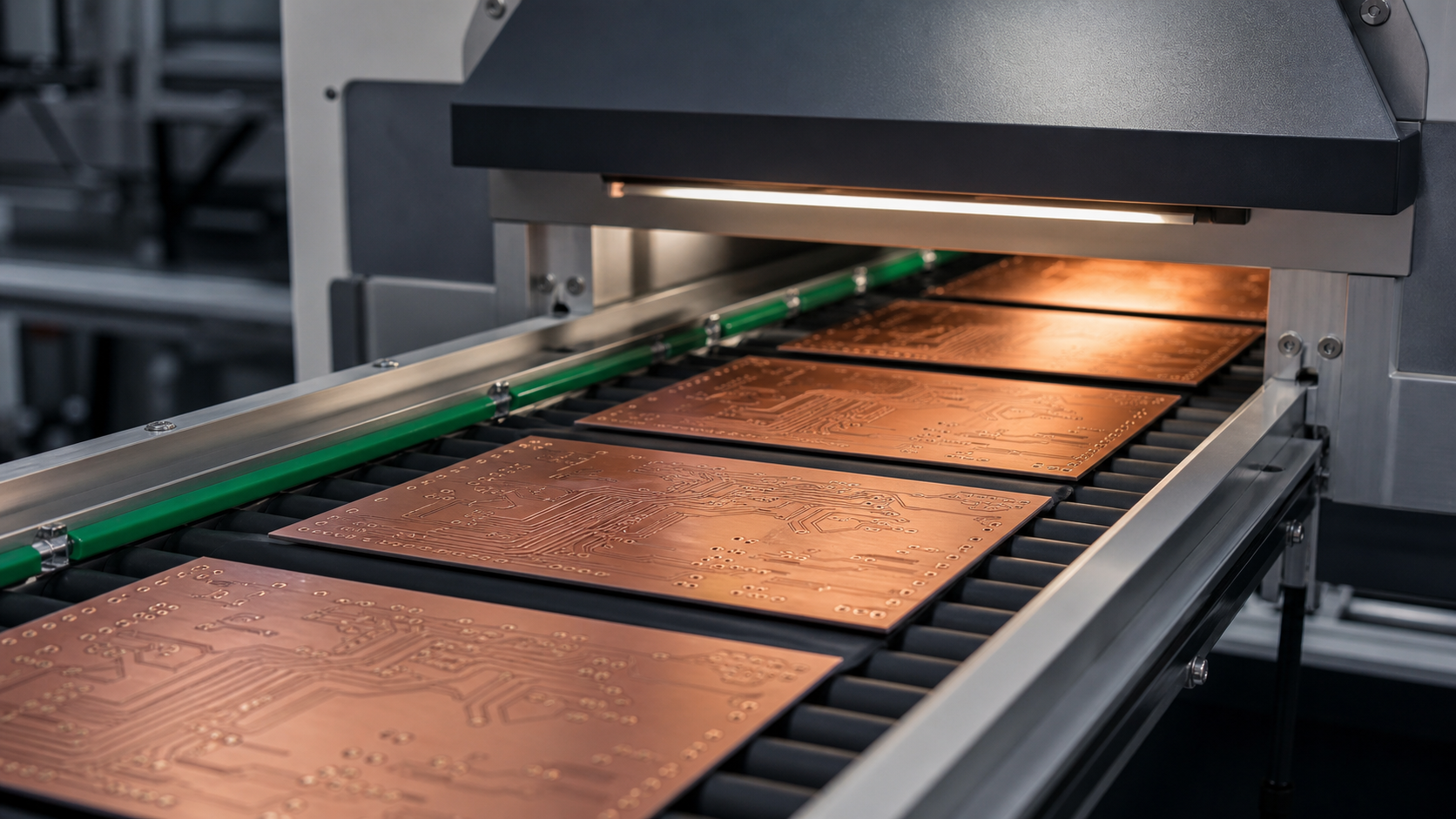
A single-sided PCB has conductive circuitry on one side of the substrate. It is often used for simple, cost-sensitive products where routing density, electrical performance, thermal demand, and test access are manageable. It is not the right default for dense controllers, high-speed signals, fine-pitch components, complex grounding, or products that need compact multilayer routing.
Where Single-Sided PCB Fits
Single-sided PCB can work well for simple power boards, LED modules, basic sensors, display accessories, low-density consumer electronics, simple chargers, and industrial interface boards. Its strength is manufacturing simplicity. Its weakness is routing limitation: without inner layers or a second copper layer, the designer has fewer routing options and may need jumpers, larger board size, or simpler circuit architecture.
IPC's IPC-2221 design standard page describes generic printed board design requirements, while IPC-6012 covers qualification and performance for rigid printed boards, including single-sided boards. Buyers do not need to quote standards in every email, but RFQs should define the acceptance basis for the actual board.
Buyer Decision Table
| Question | Single-sided PCB may fit | Consider double-sided or multilayer | |---|---|---| | Routing density | Few nets, large components, simple power paths | Many nets, fine-pitch ICs, tight board outline | | Signal needs | Low speed and forgiving layout | High speed, RF, controlled impedance | | Grounding | Simple return paths | Sensitive analog, EMI, dense digital grounding | | Test access | Test points fit on one side | Test points compete with routing | | Cost target | High volume, simple board, stable design | Cost of jumpers or larger board offsets savings |
Manufacturing Controls to Specify
Even a simple single-sided PCB needs controlled input data. The RFQ should include Gerber or ODB++ files, board outline, material, copper weight, solder mask color, surface finish, silkscreen rule, panelization preference, electrical test requirement, inspection requirement, and packing method. If the board will be assembled, add BOM, placement file, polarity marks, test requirements, programming needs, and packaging rules.
KEEP BEST connects basic PCB sourcing with PCBA manufacturing services, DFM engineering, quality management, RFQ review, technical buyer guides, and the related SMT PCB assembly process checklist.
Practical Recommendation
Use single-sided PCB when the design is simple enough that routing, thermal, test, and assembly constraints remain clean. If the design starts adding jumpers, awkward component placement, poor return paths, or hard-to-test nodes, review whether a double-sided PCB would reduce total product risk even if the bare board price is higher.
FAQ
Is single-sided PCB always cheaper?
Not always. The bare board may be cheaper, but jumpers, larger board area, awkward assembly, or weaker test access can erase the saving.
Can single-sided PCB be used for SMT assembly?
Yes, if pad layout, stencil design, component spacing, polarity, and inspection access are suitable for the assembly process.
What files should buyers send?
Send Gerber or ODB++, drill files, board outline, material notes, finish, copper weight, BOM, placement data, test needs, and target quantity.
When should buyers avoid it?
Avoid single-sided PCB for dense routing, high-speed signals, controlled impedance, sensitive analog design, complex grounding, or compact boards with many fine-pitch components.