Direct Answer
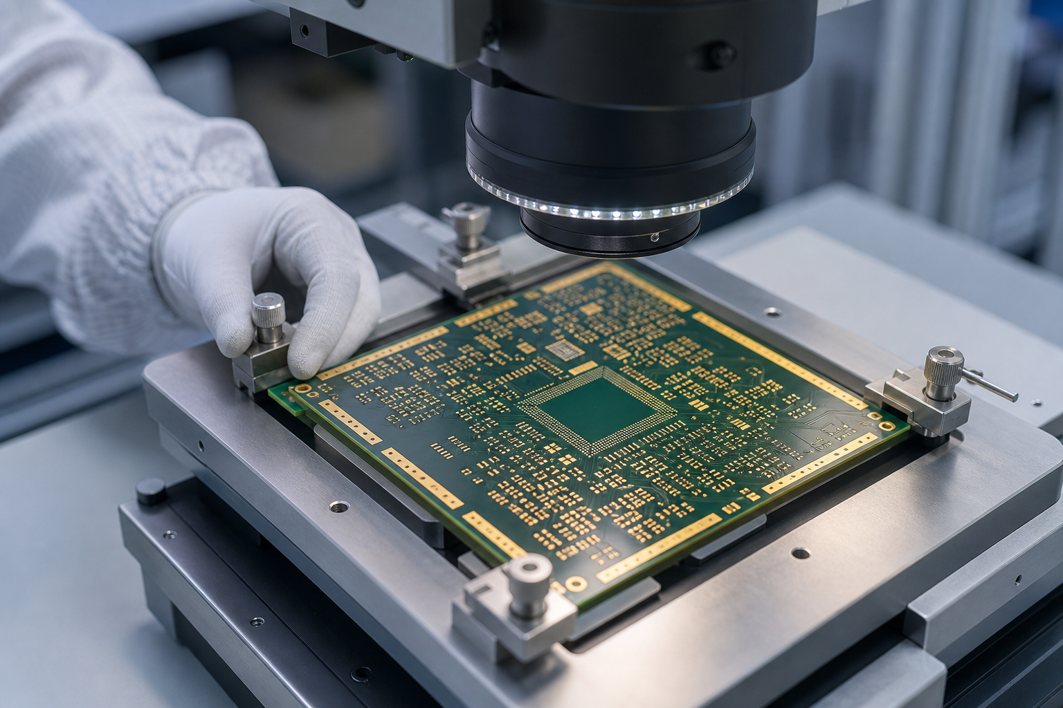
A high precision custom PCB is a purpose-built circuit board with tighter dimensional, routing, material, or reliability requirements than a standard PCB. It may involve fine-pitch pads, microvias, HDI structures, controlled impedance, unusual outline constraints, or application-specific materials. Buyers should evaluate it through manufacturability, inspection capability, and production repeatability.
Why Buyers Should Confirm This Early
The main risk is not only whether the first sample can be made. The larger question is whether the supplier can repeat the design under stable process controls. Line width, spacing, drilling, registration, solder mask alignment, surface finish, warpage, and inspection resolution all affect yield and reliability.
Buyer Checklist
| Check area | Buyer risk | Evidence to request | | --- | --- | --- | | Design limits | Fine geometry may exceed a supplier's stable process window. | Minimum line/space, via type, aspect ratio, tolerance, and design-rule review | | Material and finish | Material choice affects dimensional stability, solderability, and reliability. | Material approval, finish selection, stack-up, and alternate approval path | | Inspection capability | Small defects can escape low-resolution checks. | AOI capability, microscope or 3D inspection scope, electrical test, and defect criteria | | Production repeatability | A successful prototype does not prove lot-to-lot control. | First article report, process traveler, yield record, and deviation log |
RFQ Questions to Ask
- What minimum line width, spacing, via size, tolerance, copper weight, finish, and stack-up are assumed?
- Which design rules are outside the supplier's normal stable process window?
- How will microvias, fine-pitch pads, solder mask alignment, and electrical continuity be inspected?
- What first article, inspection, electrical test, and lot traceability records will be returned?
Supplier Red Flags
- The quote gives unit price and lead time but does not define material, process, inspection, and test boundaries.
- Alternates, rework, deviations, failed tests, and lot traceability do not have an approval path.
- First article release, in-process inspection, outgoing QA, and nonconforming material handling are unclear.
- Critical promises are not backed by a record template that can be returned with the shipment.
How KEEP BEST Connects the Work
For this type of project, buyers should connect PCBA manufacturing services, DFM engineering review, quality management, RFQ review workflow, high-precision PCB assembly risks, precision PCB supplier guide, precision sensor PCB assembly service, PCB assembly SMT risk checklist in one review path so quotation, engineering, quality, and delivery evidence stay aligned.
Practical Recommendation
Before comparing unit price, ask the supplier to mark the design limits, high-risk features, inspection plan, and lot-level records. A high precision custom PCB quote should prove repeatability, not only prototype feasibility.
FAQ
Is high precision custom PCB the same as HDI?
Not always. HDI is one common route, but high precision may also involve tight tolerances, controlled impedance, special materials, or inspection requirements.
What causes most sourcing risk?
The biggest risk is a mismatch between design ambition and the supplier's stable process window.
What evidence should a buyer request?
Request DFM feedback, stack-up confirmation, inspection scope, electrical test results, first article records, and change-control rules.